For rapid prototyping it is often useful to have circuits on a circuit board instead of a breadboard. In this post I will give a short description of how you can make your own PCB’s in a fast and cheap way with the so called Toner-Transfer Method. This process require some training, so don’t be upset if it doesn’t work the first ten times.
To develop own PCB’s you have six steps to do:
- Preprocessing
- Transfer layout
- Etch
- Postprocessing
- Drill
- Assemble
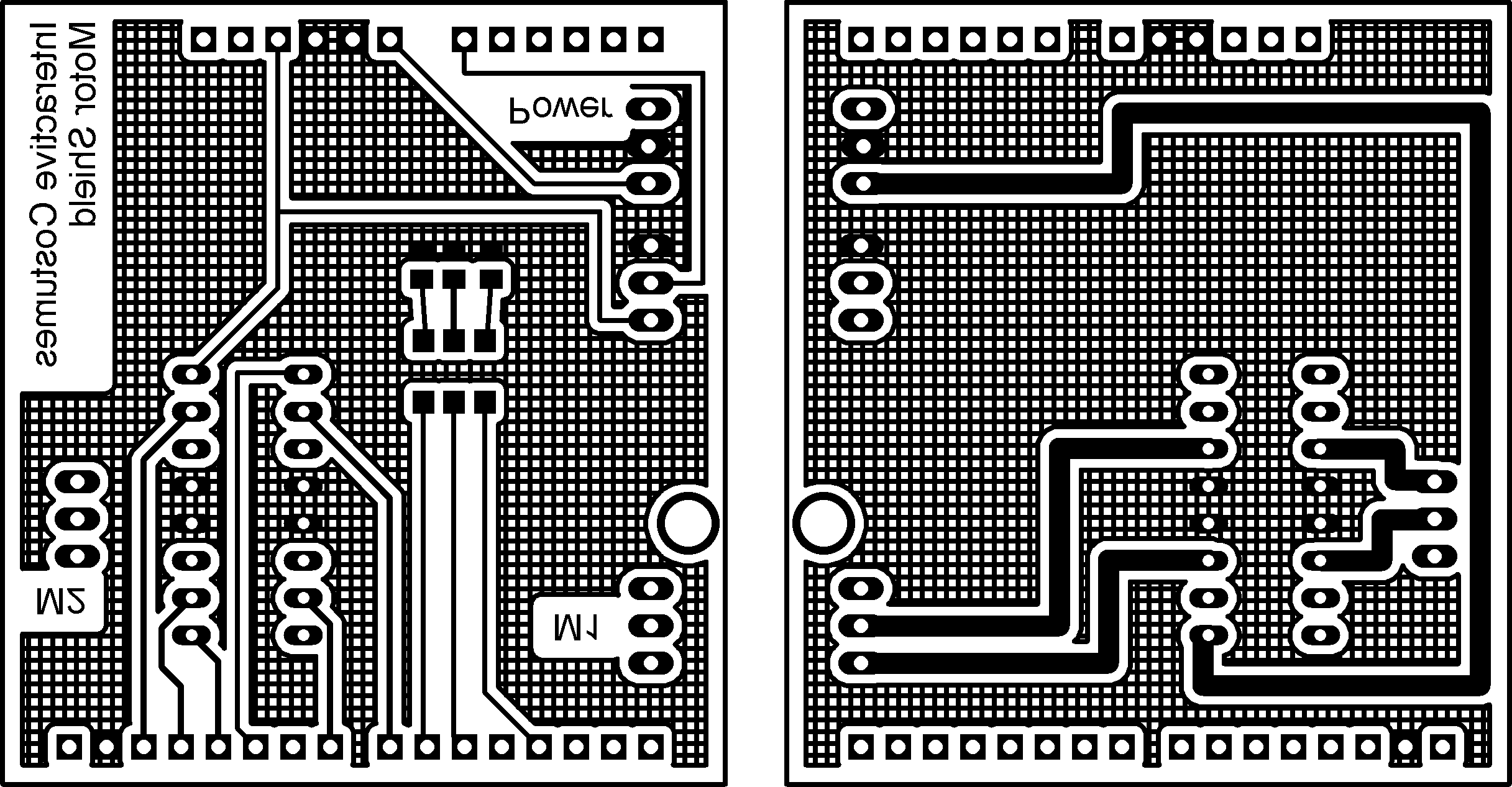
I consider that you have your schematic and board design finished with the CAD program of your choice. I will use a two-sided layout.
Preprocessing
At first export the top and bottom side of your board design as image, and arrange them next to each other. You have to mirror the top layout in order to transfer it in the correct manner onto the PCB later.
Next you have to print this image with a laser printer on a glossy paper. This prevents the toner from being soaked by the paper completely. It is advisable to print it several times to have some if it doesn’t work the first time.

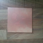
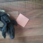
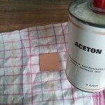
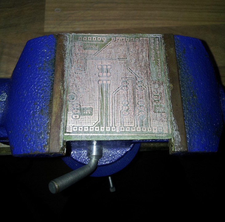
The second preprocessing step is to prepare the circuit board for the transfer. At first cut a piece of circuit board in the dimensions of your layout. Next you have to clean it really good. At first use steel wool for a rough cleaning of the board. After this use acetone to really get rid of all dirt and fat. After this procedure the copper should be shiny like a mirror. During the cleaning and transferring you should wear gloves to ensure the copper stays clean.
Transfer layout
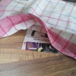
After you have your design on glossy paper and the circuit board is clean, they should come together. Because I have a two-sided layout, I have to ensure that all holes are on the same position for both sides. Therefore, you can build a small bag for the circuit board. Fold the glossy paper with the design so that both sides lie exactly on top of each other. Use duct tape to fix two other sides. Insert your circuit board from the fourth side and place it such that the design borders fit with the circuit board edges.
Now you have to transfer the design onto the circuit board. Therefore, you can use an electric iron. It is advisable to put some cotton rag between the electric iron and the paper. Adjust the electric iron to cotton temperature (This may vary with other electric irons). And start ironing the design.
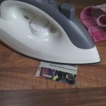
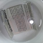
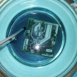
After 5 minutes the toner should be hot enough to stick to the copper. Put the (!HOT!) circuit board in a bowl with cold soap water and wait another 5-10 minutes. Then the catalog paper will dissolve. You can carefully rub over the circuit board to remove the last catalog paper.
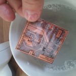
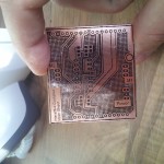
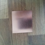
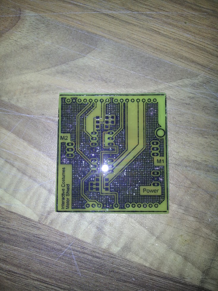
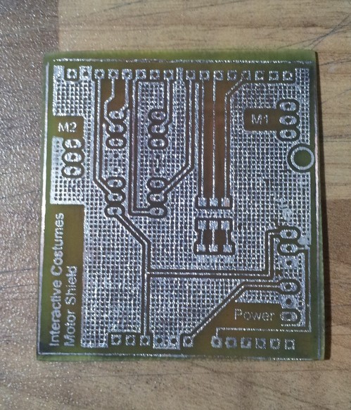
As result, you have a copper board with your design on both sides printed.
Etch
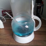
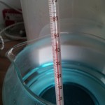
Now comes the interesting part. To etch your layout you need some Sodium Persulfate (NA2S2O8). It should have a temperature around 50°C (not more!). I use the hot plate of an old coffee maker to heat the etchant. Be careful, the etchant will make holes in fabrics, so don’t drip at your clothes (and be careful with your skin as well).
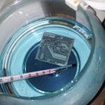
After some minutes you can see how the copper disappears from the circuit board. The toner prevents the design part from being removed by the etchant.
 Next you have to remove the toner. Therefore, you can use again acetone.
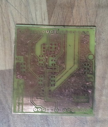
Now your circuit is on the circuit board!
Postprocessing
To prevent the copper from oxidating it is necessary to tin-coat it. For this purpose I use Rosol 3 which is available in the hardware store.
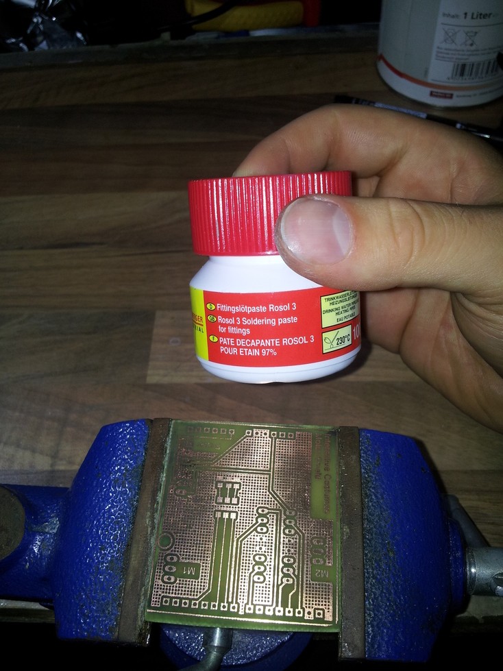
Just brush a thin layer of the Rosol 3 onto the circuit board.
Next use a heat gun to heat the tin until it starts to melt.
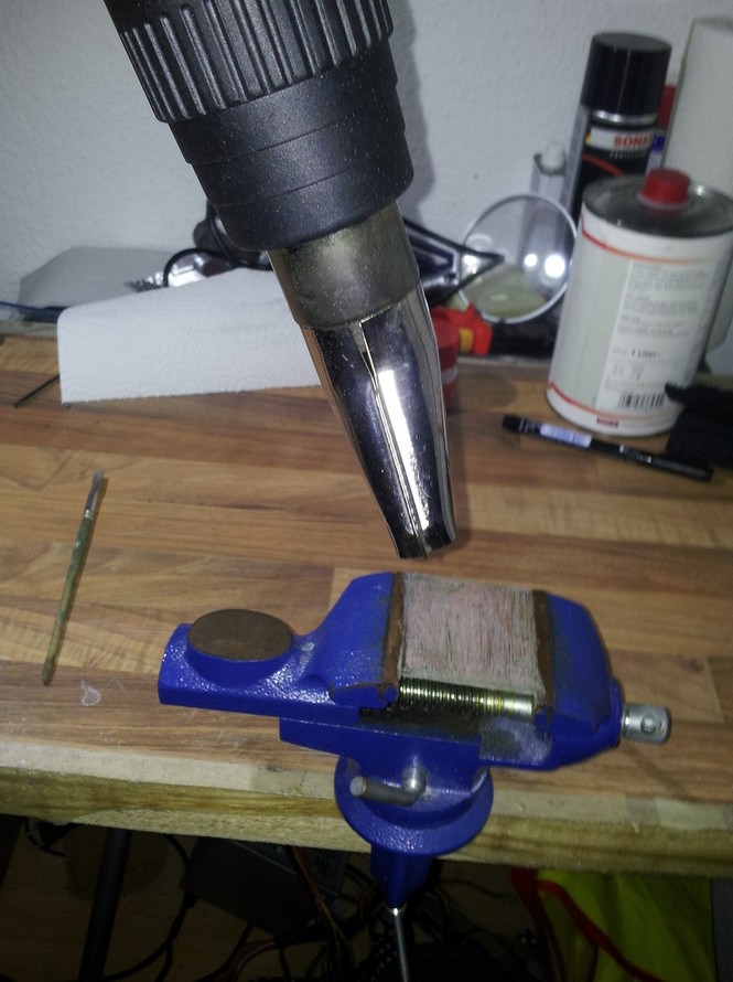
Your circuit board is now silver and protected against oxidation.
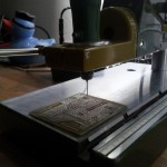
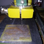
Drill
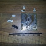
To assemble the parts to your circuit board you need to drill all the holes. I use a small Proxxon drill with drill rig. Connectors need holes with a diameter of 1.0mm, DIP packages need 0.8mm.
After this step you are nearly finished!

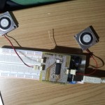
Assemble
Last but not least you have to assemble your parts and test your circuit .